


What Is a Green Device?
The word “green” has various meanings, such as the “color of leaves” and “grass.” When used in connection with the environment, as in “green” devices, it means to “sustain or protect the environment.” Devices and technologies that are effective in creating, saving or storing energy are collectively called “green devices.” Examples include solar cells and thermoelectric devices used to create energy, light-emitting diode (LED) and organic electroluminescence (EL) lighting equipment contributing to energy saving and lithium-ion rechargeable batteries that store electricity. Equipment and process technologies used to manufacture these devices also fall into the category of green devices and technologies.Recycling-Oriented, Low-Carbon Society
After the nuclear plant accident in Chernobyl in 1986, the “nuclear winter” began and persisted for several years. The winter ended in the early 1990s when a growing concern for global warming turned public attention toward nuclear power generation as a “clean” energy source that does not release CO2 and other greenhouse gases into the atmosphere. Nuclear energy, however, is expected to enter the winter season once again following the nuclear plant accident in Fukushima, which occurred in the aftermath of the Great East Japan Earthquake earlier this year, and a concern over the country’s ability to ensure stable power supply is rising. Electricity is mostly used to power motors in various machinery, followed by lighting equipment. Green devices are essential to counter power supply shortages, and such devices as energy-saving power semiconductors and LED lighting equipment as well as energy-creating solar cells have already been used in home electric appliances, automobiles and social infrastructures. In the future, we need to develop green devices and technologies that allow the efficient utilization of new, recyclable energy sources (solar light, solar heat, water, wind and biomass) and untapped energy sources (exhaust heat and vibration). A low-carbon society with less CO2 emissions must be realized by recycling energy resources.Environmentally-Friendly Semiconductors
In green devices, it is crucial to use environmentally-friendly semiconductor materials to counteract ongoing environmental pollution problems and future issues concerning the depletion of resources, in addition to providing functions to create, save and store energy. Environmentally-friendly semiconductors are semiconductor materials that are abundantly found on earth and have minor toxicity to the human body and the environment. Our Optobioelectronics Lab is engaged in the development of materials and process technologies for environmentally-friendly semiconductors, using silicon, gallium, aluminum and iron as well as nitrogen, oxygen and other elements found in the atmosphere. Examples of such materials include beta-iron disilicide (solar cells and thermoelectric devices) and nanocrystalline silicon, aluminum nitride and gallium nitride (LED) (Figure 1).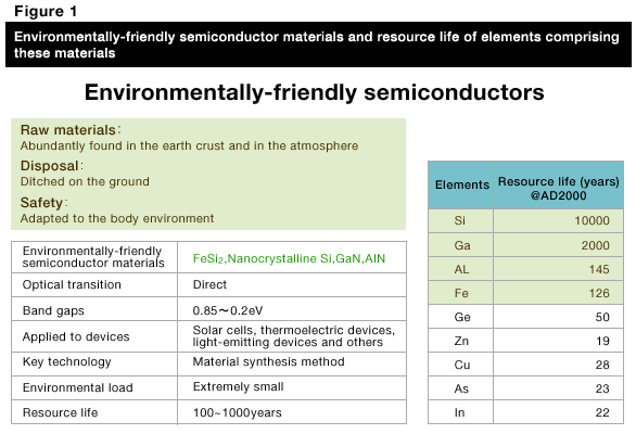
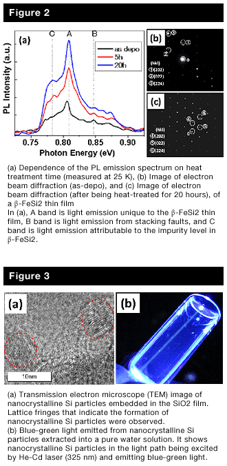
Figure 2 shows the optical and structural characteristics of a beta-iron disilicide thin film synthesized by vacuum electron-beam evaporation of iron on a silicon substrate. As seen from the figure, the crystalline structure of the beta-iron disilicide thin film improves after undergoing 20 hours of heat treatment, resulting in increased luminescence intensity in the 1.5 μm band. Layered structures consisting of high-quality beta-iron disilicide thin films and silicon films are expected to increase the efficiency of silicon solar cells. Figure 3 shows an electron beam diffraction pattern of a sample (silicon nanocrystals with a diameter of less than 10 nm formed within a silicon dioxide film by sputtering) and an example observation of luminescence from a solution sample (silicon nanocrystals extracted into pure water). Silicon does not emit light in the visible spectrum, but when turned into nanocrystals, it emits blue-green light. As described above, we can create a visible light-emitting device from silicon, which is available in abundance and has only minor toxicity to the ecological environment, by using low cost, environmentally friendly processes.
In Japan, many companies have been making concerted efforts to add “green” functions to their products, namely electrical appliances, by working to improve individual devices and materials. Green devices thus represent a technical field in which Japan can demonstrate its technological superiority. In the future, green devices will gain increased importance in terms of protection of the global environment and simultaneously form another industrial field that will lead the future global economy, with their applications extending into the agricultural, automobile and other industries.
Profile
Associate Professor of Department of Electronics and Bioinformatics, School of Science and Technology, specialized in semiconductor device and process engineering.Born in Kanagawa Prefecture in 1969. Graduated from Department of Electrical Engineering, School of Technology, Meiji University in 1992. Earned Ph. D. (Engineering) at Graduate School of Science and Technology, Meiji University in 1997. Served as a lecturer (research institute researcher) in the Ion Beam Engineering Experimental Laboratory, Faculty of Engineering, Kyoto University from 1997 to 2000. Worked for the Process Research Center within the Corporate Manufacturing Engineering Center of Toshiba Corporation from 2000 to 2010. Assumed current position in 2010.
Major Research Paper
“Fabrication of Heterostructure p-β-Fe0.95Mn0.05Si2/n-Si Diodes by Fe+ and Mn+ Co-implantation in Si(100) Substrates,” Thin Solid Films, Volume 381, pp. 244 - 250, 2001“The Effect of Crystalline Structure on Photoluminescence of the β- FeSi2 Film Prepared by Pulsed Laser Deposition Using Two Types of Target,” Physics Procedia, Volume 11, pp. 158 - 162, 2011


